1. Customization of sensors and specifications for customers’ inspection needs
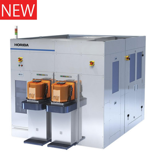
"Xtrology," is a highly customizable system that allows you to select one or multiple sensors from three analysis methods: spectroscopic ellipsometry*2, Raman spectroscopy*3, and photoluminescence*4. This has made it possible to perform important inspections of various wafers with a single instrument.
■Main measurement solutions
■Available sensor examples
2. Automatic measurement technology contributes to improved efficiency and yield
It not only has an automation function that combines our in-house developed automatic conveyance system and non-destructive, non-contact sensors, but also connects multiple external devices, such as open cassettes*8, SMIF*9, and FOUP*10. Continuous measurements can be performed, contributing to more efficient inspection processes and higher yields.
3. Consistent support system because of in-house development
Because HORIBA has developed all of the sensors, automation technology, and software installed in this device in-house, we are able to provide consistent services and maintenance. Having 29 countries and regions around the world in operations, HORIBA provides long-term global support.
*1 The appearance will vary depending on the number, type, and specifications of the sensors installed. (The picture is 2 different sensors installed with multi-ports)
*2 An analysis method that determines the thickness and properties of a sample by measuring changes in the vibrations of light incident on the sample and reflected light
*3 An analysis method that evaluates molecular structure and properties by irradiating a sample with light and detecting the scattered light
*4 An analytical method that obtains information on defects and impurities by absorbing light at a specific wavelength and measuring the light (fluorescence) emitted by the sample
*5 An indicator of how weak light becomes when passing through a substance
*6 Width of region where electrons cannot exist
*7 The force that occurs inside an object when it receives a force from the outside
*8 Open storage pod used when high cleanliness is not required
*9 Abbreviation for Standard Mechanical Interface. Closed storage pod used to transport wafers in semiconductor manufacturing
*10 Abbreviation for Front Opening Unified Pod. Storage pod used to transport and load 300mm wafers into the equipment


